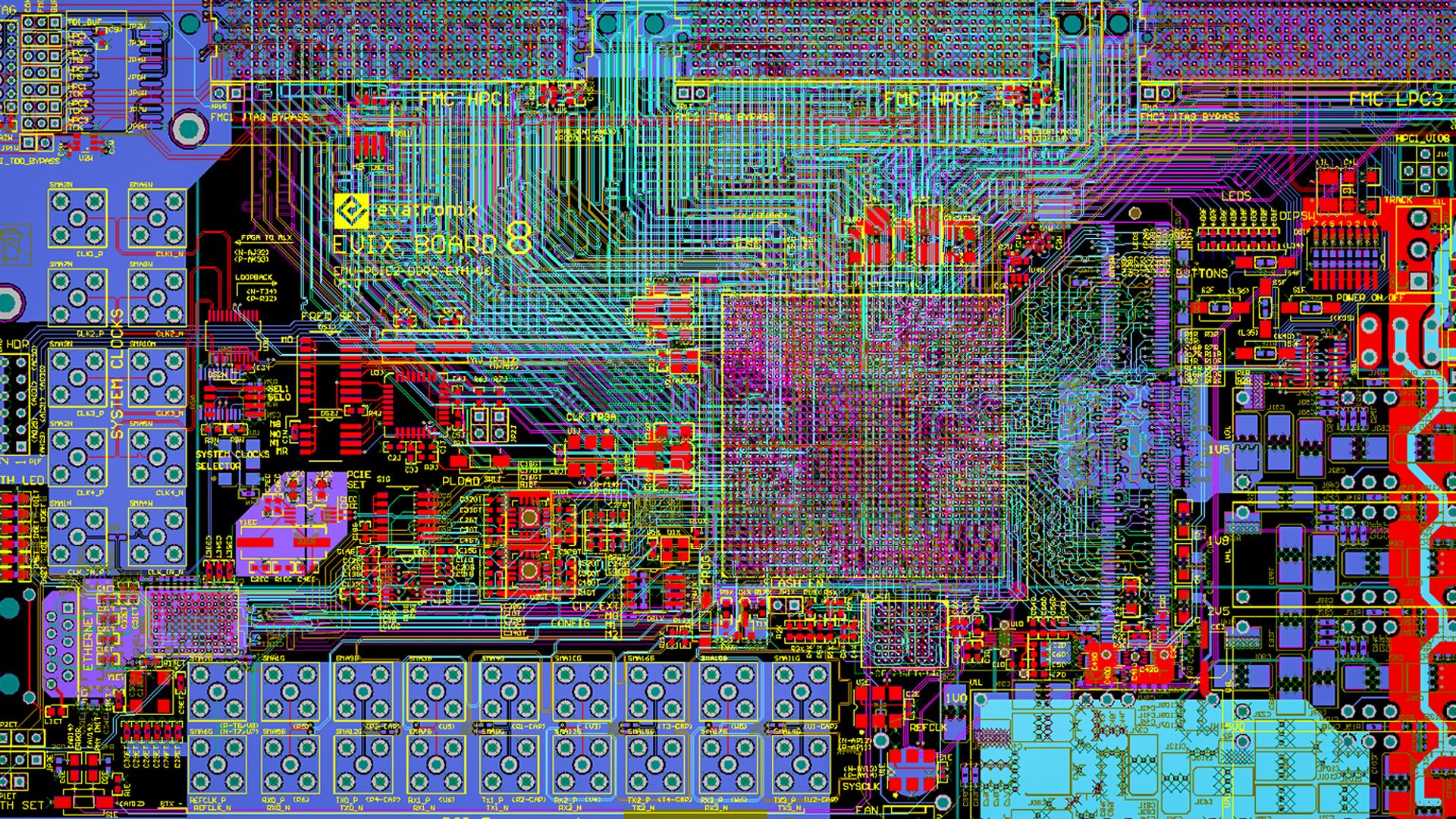
PCBs are essential because they provide the design blueprint for your circuit system. They tell your electrons where to go and where not to go. So why should you care about pcb design and development? Because there is no electronic device that does not have printed circuit boards in them.
How is PCB Designed and Developed?
There is a process of PCB Designing and Development which is as under
- Knowing the requirement of the circuit to be made and selecting the components for development.
- Designing a PCB layout through a particular PCB Design Software.
- Running the Design for Manufacture (DFM) before the circuit fabrication starts.
- Printing on the copper layers of the panel is done.
- Remove unwanted copper through the alkaline solution.
- Punching on all inner and outer layers and holes is made.
- To prevent errors in the inner layers of the panel automated optical inspection process is done before bonding and lamination.
- Bonding of layers with an aluminum press plate.
- We are drilling on PCB Panel to create holes.
- Copper layering covers the non-conductive materials and extra holes seen after drilling PCB Panel.
- Cleaning of PCB panel for application of soldering mask that creates green color on the panel.
- To check the overall performance electric test on a circuit is done.
- Final visual and quality inspection helps to check boards’ physical damage.
Printed circuit boards (PCBs) are a significant part of the design of any electronic device. They have been the backbone of electrical systems since the transistor’s invention.

